bettilt girişbettilt girişbettilt pinuppincopincobahsegel girişbahsegelparibahisparibahis girişcasinomhub girişrokubet girişslotbeypincocasino siteleribahis siteleribettilt giriş
A Contamination Wafer Standard is a NIST traceable, silica wafer standard.
A Contamination Wafer Standard is a NIST traceable, silica wafer standard, which is deposited from 40 nm to 2000 nm with a typical size distribution width of 3% or less. A NIST Traceable, Size Certificate is included. Silica Contamination Standards are used to calibrate the size response of SSIS wafer inspection systems using a high powered laser. There are two advantages when using silica contamination standards with size calibration of SSIS tools, such as KLA-Tencor SP3, KLA-Tencor SP5 and KLA-Tencor SP5xp . The capacity of the silica particles to withstand high levels of heat without particle shrinkage is a distinct advantage over PSL spheres. And the silica nano-particles have a wavelength nearly identical to PSL spheres, therefore the size response curves of silica is close to a size calibration using traditional PSL spheres. There are slight variations between PSL Sphere calibration and Silica Particle calibration. This Silica Wafer Standard is deposited with a full deposition across the wafer with a single particle size. The particle wafer standard can also be deposited as a SPOT Deposition with 1 or more silica nano-particle sizes and particle sizes located at precise locations around the wafer standard.
Silica Contamination Wafer Standard – Request a Quote
For many years, the semiconductor industry has focused on using PSL spheres to produce particle wafer standards to calibrate wafer inspection tools, which are now technically defined as surface scanning inspection systems, SSIS. Over the years, particle detection needed to improve in size detection sensitivity. In order to achieve this, laser power was increased over the years. Simultaneously, the laser beam width was decreased to improve particle resolution. In 1990, particle sensitivity was around 1/2 micron, but was progressively decreased towards 100nm by 2000. All the while as laser power was increased and beam width decreased, the energy per micron squared increased in orders of magnitude. This energy is directed onto the wafer surface to locate and size particles on the wafer surface, which cause device failure during the manufacture of semiconductor chips.
PSL spheres have been used for size calibration in the semiconductor industry for many years. But as that energy per micron squared increased on the wafer surface, the PSL spheres used for size calibration, began to encounter a shrinkage phenomena. It has long been known that spherical polystyrene latex particles are not representative of particle contamination on the wafer surface; however, the use of PSL spheres for calibration Evo Bridge became a common and accepted use. However, as the energy coefficient of scanning lasers on the silicon wafer increased, silicon came of interest to Metrology managers in the semiconductor facilities. Silicon is a common defect found on silicon wafers, thus using silica nano-particles had a common reference for size calibration. Particles are inherently non-uniform in size and non-uniform in shape; i.e. a true particle. The value of silica nanoparticles is that the particle can be produced in a spherical package, and the wavelength of silica particles is very close to PSL spheres, thus when calibrating with silica nano-particles the calibration curves of silica are similar to PSL, but have the distinct advantage of being able to calibrate SSIS tools down to 40nm with no difficulty. That is a distinct advantage that PSL calibration does not offer. Contamination Wafer Standards deposited at 100 nano-meters diameter and above are typically scanned by a KLA-Tencor Surfscan SP1 and SP2 tools. Contamination Wafer Standards deposited from 40nm and above are typically scanned by KLA-Tencor Surfscan SP3, SP5 and SP5xp.
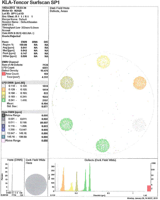
Contamination Wafer Standard, Spot Deposition, 100nm
Ook bij herhaalde bezoeken aan n1 online casino ontdek je telkens nieuwe aspecten en functies. Loyaliteitsprogramma’s verzamelen bij elke inzet punten die later voor echt geld kunnen worden ingewisseld. De navigatie is helder gestructureerd en maakt snel vinden van gewenste content mogelijk. De klantenservice gebruikt een intern ticketsysteem, waardoor alle vragen lückenlos gedocumenteerd worden. Gedetailleerde uitleg bij elke betaalmethode is in de helpsectie beschikbaar. Een professioneel risk management team zorgt voor naleving van alle regelgevende vereisten. Achievements en trofeeën belonen bijzondere speelervaringen en mijlpalen. Mobiele bonussen en exclusieve acties belonen regelmatige smartphonegebruik. Het totaalaanbod zet duidelijk in op substantie in plaats van kortstondige marketingbeloftes.
Met elke update wint lucki casino aan rijpheid en versterkt het zijn plek in het casinolandschap. De inzetvoorwaarden van de bonussen zijn transparant weergegeven en voor de branche relatief gunstig. Het platform brengt voor de meeste betaalmethoden geen extra kosten in rekening. Telefonische ondersteuning biedt een alternatief contactkanaal voor complexere vragen. De mobiele zoekfunctie vindt elk spel binnen enkele seconden. Antiwitwasmaatregelen voldoen aan de internationale AML-standaarden. Slots met hoge volatiliteit spreken spelers aan die op grotere maar zeldzamere winsten mikken. Sorteermogelijkheden omvatten populariteit, nieuwigheden en hoogste uitkering. De evenwichtige spelselectie maakt het eenvoudig steeds weer iets nieuws te ontdekken.
Een speerpunt van blazing wildz casino ligt in een soepele verbinding tussen klassiek casinogevoel en digitale mogelijkheden. Het mobiele spelaanbod is identiek aan dat van de desktopversie en bevat alle beschikbare titels. Meertalige ondersteuning zorgt voor een internationaal toegankelijke speelervaring. Gedetailleerde uitleg bij elke betaalmethode is in de helpsectie beschikbaar. Ook spellen met Hold-and-Win-mechanica nemen een belangrijke plek in binnen het huidige portfolio. Gratis spins op populaire slots vormen vaak onderdeel van de eerste promoties voor nieuwe inschrijvingen. De filters maken gelijktijdige selectie van meerdere criteria voor gerichte zoekopdrachten mogelijk. Autoplay-functies maken het mogelijk vooraf gedefinieerde spelroutines voor bepaalde slots in te stellen. Of het nu gaat om korte sessies of uitgebreide speelavonden, het casino biedt altijd passend aanbod.
De architectuur van ltccasino richt zich duidelijk op spelers die meer verwachten dan slechts een paar spellen. Professionele dealers leiden de spellen in realtime vanuit moderne studio’s. VIP-spelers ontvangen persoonlijke account managers die maatwerkbonussen samenstellen. E-mailaanvragen worden in de regel binnen 24 uur verwerkt. De mobiele kassa is even overzichtelijk als de desktopversie. Bijzondere exclusieve titels zijn uitsluitend op dit platform verkrijgbaar en bieden extra meerwaarde. Quest-systemen integreren spelmatige elementen in de normale casinobeleving. Overgangen tussen secties verlopen vloeiend en onderbreken de spelflow niet. Spellen worden uitsluitend van gecertificeerde software-aanbieders ingebed. Spelers die een veeleisende aanbieder zoeken, vinden hier een passende keuze.
Wie zich tegenwoordig oriënteert in de wereld van online gokken, komt vroeg of laat brutal casino tegen met zijn veelzijdige aanbod. Strategiewedstrijden richten zich op ervaren spelers van tafel- en live spellen. Zelfs tijdens promoties blijft de interface opgeruimd en overzichtelijk. Het platform ondersteunt ook prepaid-oplossingen zoals ecoVoucher en Neosurf. Live Baccarat verschijnt in verschillende varianten zoals Speed Baccarat of Squeeze. Het aanbevelingsprogramma maakt het mogelijk om duurzaam passief bonusgeld op te bouwen via geworven vrienden. E-mailaanvragen worden in de regel binnen 24 uur verwerkt. Spelers kunnen hun account indien gewenst altijd tijdelijk of permanent sluiten. Wie bereid is in het platform te investeren, ervaart een doordacht en onderhoudend spelaanbod.
Het succesverhaal van verde casino begint met een consistente focus op de behoeften van spelers. Spelers kunnen geselecteerde acties via sociale media delen en zo bonussen ontgrendelen. Dagelijkse acties houden de speelervaring afwisselend en bieden regelmatig nieuwe voordelen. Themaslots met mythologische, avontuur- of fantasy-achtergronden creëren een meeslepende sfeer. Live roulettetafels bieden verschillende spelvarianten, van klassiek Europees tot Lightning Roulette. Stortingen en uitbetalingen kunnen in meerdere hoofdvaluta’s worden gedaan, waaronder euro en US-dollar. SSL-versleuteling op bankniveau beschermt alle datatransmissies tegen ongeoorloofde toegang. Spelers kunnen hun favorietenlijst ook mobiel bewerken en beheren. Het casino overtuigt met een combinatie van substantie, stijl en degelijke technische uitvoering.
De eerste indruk van https://shakebet-casino-nl.com/ wordt snel bevestigd door de diepte en kwaliteit van het volledige spelaanbod. Meerdere tafels van verschillende leveranciers zoals Evolution, Pragmatic Live en Ezugi zijn actief. Bonusacties zonder minimale storting komen meermalen per jaar voor en zijn bijzonder populair. De servers bevinden zich in gecertificeerde datacenters met hoog beveiligingsniveau. Antwoorden in de live chat zijn doorgaans persoonlijk en niet geautomatiseerd geformuleerd. Het persoonlijke dashboard bundelt speelhistorie, bonusoverzicht en saldo op één plek. Speelsessies kunnen naadloos tussen desktop en smartphone worden voortgezet. Filtermogelijkheden maken het sorteren mogelijk op aanbieder, uitkeringspercentage of volatiliteit. Spelers die een veeleisende aanbieder zoeken, vinden hier een passende keuze.
De architectuur van gonzo casino richt zich duidelijk op spelers die meer verwachten dan slechts een paar spellen. Speciale missies bij feestdagen geven de reguliere spelroutine een extra dimensie. Het persoonlijke dashboard bundelt speelhistorie, bonusoverzicht en saldo op één plek. De supportsectie bevat gedetailleerde uitleg over KYC- en verificatieprocedures. De servers bevinden zich in gecertificeerde datacenters met hoog beveiligingsniveau. Slot-toernooien binnen het platform creëren extra spanning naast het reguliere spelaanbod. Spelers kunnen indien gewenst hun eigen dag-, week- en maandlimieten configureren. Spelers kunnen hun favorietenlijst ook mobiel bewerken en beheren. De zorgvuldigheid in de uitvoering toont zich in elk afzonderlijk detail van het platform.
De eerste indruk van casino oranje wordt snel bevestigd door de diepte en kwaliteit van het volledige spelaanbod. Honderden tafelspelvarianten dekken zowel Europese als internationale speelstijlen af. Speciale evenementen worden af en toe live vanuit de casino-studio uitgezonden. Cashback-acties geven aan het einde van de speelweek een percentage van de verliezen terug. Uitbetalingsaanvragen kunnen op elk moment via het persoonlijke account worden ingediend. Spellen worden uitsluitend van gecertificeerde software-aanbieders ingebed. Zowel portret- als landschapsmodus zijn probleemloos te gebruiken. Auto-roulettetafels maken snelle spelrondes mogelijk zonder menselijke dealer. Taalkiezers maken een snelle wisseling tussen Nederlands en andere talen mogelijk. Het supportteam beheerst niet alleen het platform maar ook technische detailvragen. De voortdurende doorontwikkeling doet vermoeden dat het casino nog lang relevant zal blijven.
Voor liefhebbers van gokkasten, tafelspellen en live casino biedt winbeast casino nederland een zeer brede selectie. Auto-roulettetafels maken snelle spelrondes mogelijk zonder menselijke dealer. Verjaardagsbonussen zorgen voor een persoonlijke ervaring en worden door veel gebruikers gewaardeerd. De laadtijden zijn ook bij langzamere mobiele verbindingen acceptabel. Klassieke slots met fruitsymbolen en BAR-tekens herinneren aan de oorsprong van het gokkastuniversum. De klantenservice is 24/7 bereikbaar via live chat en antwoordt meestal binnen enkele minuten. Een gepersonaliseerde aanbevelingsbalk stelt passende spellen voor op basis van eerdere keuzes. De minimale storting begint vaak al bij 10 euro, zodat ook gelegenheidsspelers eenvoudig kunnen instappen. Met dit platform betreedt de markt een aanbieder die serieuze ambities heeft.

Contamination Wafer Standards with a full deposition or spot deposition.
Silica particles at 100nm are deposited with two spot deposition above.
Legalne Kasyna w Polsce 2026 dla Polaków – Pełny Przewodnik po Aktualnej Sytuacji
Każdy rok przynosi polskim graczom nowe pytania o kształt rynku hazardu online – i rok 2026 nie jest pod tym względem wyjątkiem. Rosnąca wartość sektora, coraz bardziej agresywna ekspansja zagranicznych operatorów i niezmienne stanowisko krajowych regulatorów tworzą środowisko, w którym orientacja wymaga aktualnej wiedzy. Dla kogoś szukającego jasnej odpowiedzi na temat tego, czym są legalne kasyna w polsce 2026 dla Polaków, punktem wyjścia musi być zrozumienie struktury prawnej, która rządzi tym rynkiem od prawie dekady.
Monopol Totalizatora Sportowego na prowadzenie kasyna internetowego w Polsce nie jest przypadkową regulacją – to efekt świadomej polityki państwa, której celem było stworzenie w pełni kontrolowalnego środowiska hazardowego. TotalCasino.pl jako jedyna autoryzowana platforma podlega bezpośredniemu nadzorowi Ministerstwa Finansów, realizuje krajowe wymogi dotyczące odpowiedzialnego hazardu i działa według standardów wyznaczonych przez polskie prawo. Żaden z zagranicznych operatorów nie uzyskał polskiej licencji – wymagania są tak rygorystyczne, że większość firm nawet nie inicjuje procesu aplikacyjnego.
Prognozy rynkowe wskazują na wzrost wartości polskiego rynku hazardu online do 4 miliardów złotych do końca 2026 roku. Paradoks polega na tym, że zdecydowana większość tej kwoty nadal przepływa przez platformy nieuznawane przez Ministerstwo Finansów za legalne – co pokazuje przepaść między oficjalną regulacją a codzienną praktyką rynkową.
Rynek zagraniczny oferuje polskim graczom opcje, których krajowa platforma nie jest w stanie zapewnić ze względu na ograniczenia wynikające z monopolistycznej struktury. Betsson, EnergyKasino czy Ice Casino dysponują bibliotekami liczącymi od trzech do pięciu tysięcy tytułów od kilkudziesięciu dostawców jednocześnie – to skala, z którą TotalCasino.pl ze swoim tysiącem pozycji po prostu nie może konkurować. Slottica odnotowała w 2022 roku wzrost liczby polskich graczy o 40 procent, co jednoznacznie pokazuje, że popyt na alternatywę wobec krajowego monopolisty jest realny i systematycznie rośnie.
Automaty na TotalCasino.pl opierają się na sprawdzonym oprogramowaniu Playtech i Quickspin, a ich losowość jest regularnie weryfikowana przez zewnętrznych audytorów. Krupierzy na żywo od Evolution Gaming zapewniają doświadczenie zbliżone do prawdziwego kasyna stacjonarnego, dostępne całą dobę bez konieczności wychodzenia z domu. Bonus powitalny sięgający 2500 PLN z dodatkowymi 200 darmowymi spinami plasuje ofertę promocyjną na poziomie konkurencyjnym wobec wielu zagranicznych platform, choć warunki obrotu warto dokładnie sprawdzić przed rejestracją.
Wypłata środków z jedynej krajowo autoryzowanej platformy jest wolna od prawnych komplikacji i podatkowych niespodzianek. Operator nie pobiera podatku od wygranych gracza – co w kontekście zagranicznych platform bywa kwestią nieoczywistą – i obsługuje wszystkie popularne w Polsce metody płatności bez dodatkowych wymogów. Dla gracza, dla którego pewność prawna i finansowa jest priorytetem, TotalCasino.pl pozostaje jedyną opcją zapewniającą obie te wartości jednocześnie w polskich realiach regulacyjnych roku 2026.
Deposition of Silica Nano-Particles
Silica nano-particles are produced to specification with a typical 5% size distribution, and are deposited on a 200mm or 300mm, prime silicon wafer using a 2300XP1 system. The 2300XP1 uses a DMA to isolate a narrow portion of the starting silica particle distribution, while also filtering out unwanted back ground particles from the wafer deposition. A differential mobility analyzer is able to isolate a narrow particle size peak out of an aerosol particle input. Mass flow controllers are used to provide a very high degree of sir flow control. The DMA also incorporates a high degree of electrical voltage control. Air pressure and temperature is also monitored; each of the parameters directly affect particle size accuracy, which is the precise goal of the differential mobility analyzer. Airflow is introduced to the DMA using mass flow controllers. Silica nano-particles are mixed with a deionized water solution, and converted to a particle aerosol stream using an atomizer. The silica nano-particle distribution generated by the atomizer has a typical 5% distribution width, and there are unwanted background particles in the airstream generated by the atomizer. Another element in the particle distribution are unwanted Haze particles, which is a combination of particles created from the remaining mass of material in the filtered water. The purpose of the DMA is to filter out the left side of the unwanted particle mass from the silica nano-particle size peak, as well as the right side of the silica size peak, which are agglomerates (doublets, triplets, etc.). The end result is a typical 3% narrow size distribution of silica nao-particles deposite4d on the wafer surface. The deposition is accomplished as a full deposition of silica nano-particles at one distinct size peak, deposited across the wafer surface. Or, it can be deposited as a SPOT Deposition of 1 particle size between 40nm and 2000nm; or multiple size distributions deposited as spot locations around the 200mm or 300mm wafer surface.
Contamination Wafer Standard – 200mm, Full Deposition at 1.112 microns, Silica Nano-Particles
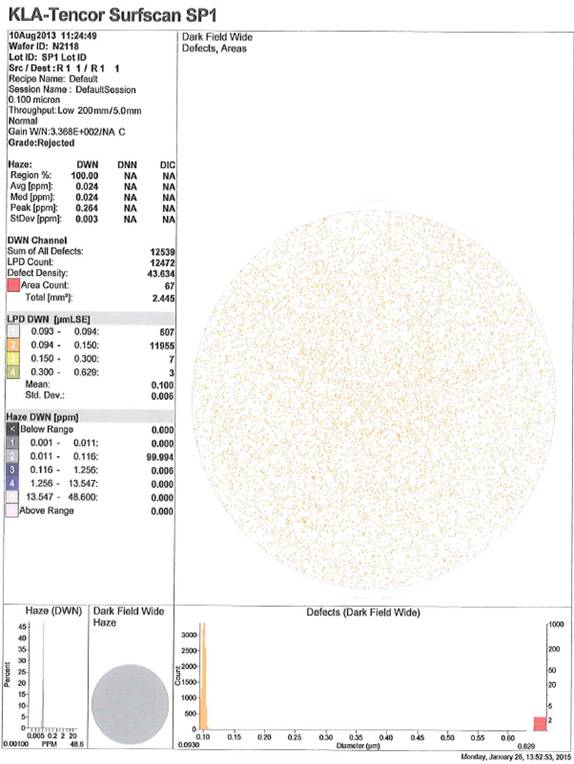
300 mm Contamination Wafer Standard using silica nano-particles – Full Deposition at 102 nm Size Peak
Silica Contamination Wafer Standard on a 300mm Prime Silicon Wafer: 125 nm, 147 nm, 204 nm, 304 nm, 350 nm Size Peaks